
 Product
 Brand
Brand Articles
 Tools
Tools
The Introduction to QFN Package
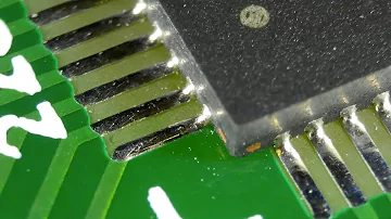
SMD Soldering - QFN Package
Topics Covered in This Article: |
Ⅰ. What is a QFN Package? |

Ⅰ. What is a QFN Package?
The Quad Flat No-leads (QFN) package is a type of surface-mount technology (SMT) that has become a cornerstone of modern electronics due to its compact size and excellent performance. Unlike older packages like the Quad Flat Package (QFP) or Plastic Leaded Chip Carrier (PLCC), the QFN has no external leads (or "gull wings"). Instead, it features metal pads, known as "lands," on the underside of the package for electrical connection.
The four sides of the package are equipped with these electrode contacts. This leadless design results in a smaller mounting area and a lower profile compared to QFP. QFN packages are typically made from ceramic or plastic. Plastic QFNs, often built on a glass-epoxy substrate, are a cost-effective solution with common electrode contact pitches of 0.65mm and 0.5mm. The term QFN was originally defined by the Japan Electronics and Information Technology Industries Association (JEITA).

Ⅱ. Key Features and Advantages
The QFN package is distinguished by a large exposed pad in the center of its bottom surface. This pad serves as a thermal connection, providing a direct path for heat to dissipate from the chip to the printed circuit board (PCB). The short conductive path between the internal die and the external pads results in very low self-inductance and wiring resistance, granting it superior electrical performance, especially for high-frequency applications.
These characteristics—small size, light weight, and outstanding electrical and thermal properties—make QFN packages ideal for any application where size and performance are critical. For instance, a 32-pin QFN (5x5mm) can reduce the footprint by 84% and thickness by 80% compared to a traditional 28-pin PLCC. This miniaturization is a key reason for its rapid adoption in mobile phones, digital cameras, automotive electronics, and IoT devices. The global QFN package market was valued at approximately USD 278 million in 2024 and is projected to continue its steady growth, driven by these high-demand sectors.

Ⅲ. PCB Design for QFN Packages
Proper PCB design is critical for leveraging the full potential of QFN packages. While early designs often referenced the IPC-SM-782 standard, the more modern IPC-7351 series is now the primary industry guideline for land pattern design. Key design considerations include the peripheral pads, the central thermal pad, and the solder mask.
Thermal Pad and Via Design
To effectively transfer heat, the PCB must have a corresponding thermal pad and thermal vias directly beneath the QFN's exposed pad. The vias create a pathway for heat to dissipate into the ground planes of the PCB. A typical via array pattern uses a 1.0mm to 1.2mm pitch with via diameters of 0.3mm to 0.33mm. Vias can be tented, filled, or left as open through-holes, each method offering trade-offs in voiding and solder flow.

Stencil Design
Stencil design is crucial for achieving reliable solder joints. For the central thermal pad, it is recommended to use an array of smaller openings (a "windowpane" design) instead of one large opening. This approach helps reduce solder voiding by allowing gases to escape during reflow. A solder paste coverage of 50% to 80% is typical. For peripheral pads, the stencil aperture is usually designed to be slightly smaller than the pad to prevent solder bridging, especially for fine-pitch (≤0.5mm) components.

Ⅳ. The Evolution of QFN Technology
The basic QFN package has evolved into several variants to meet increasingly demanding application requirements:
WQFN (Very-thin QFN): An even thinner version of the package, often with a finer pitch (e.g., 0.35mm), allowing for a higher I/O count in a smaller area.
FC-QFN (Flip-Chip QFN): This variant uses flip-chip interconnects, which dramatically shorten the signal path (<100 µm). This is ideal for high-frequency applications like millimeter-wave (mmWave) radar and 5G antennas.
SiP-QFN (System-in-Package QFN): Integrates multiple dies and/or passive components into a single QFN package, creating a complete subsystem in a tiny form factor.
Wettable Flank QFN: Features a special plating on the side edges of the pads. This creates a visible solder fillet after reflow, which is crucial for automated optical inspection (AOI) and is often a requirement in the automotive industry.
Ⅴ. Solder Joint Inspection and Rework
Inspection
Inspecting QFN solder joints is challenging because the primary connections are hidden beneath the package. While Automated Optical Inspection (AOI) can check for peripheral issues like solder bridging, it cannot see the crucial joints on the pads. This is where Automated X-ray Inspection (AXI) becomes essential. AXI can verify the integrity of the solder joints on the I/O pads and, critically, assess the level of voiding in the central thermal pad. The development of wettable flank QFNs has also been a major step forward, as it allows standard AOI systems to verify soldering on the package's perimeter.

Rework
Reworking QFN components is a delicate process, similar to that for Ball Grid Arrays (BGAs). Defects like bridges, opens, or excessive voiding require the component to be removed. This is typically done using specialized hot-air rework stations that can apply focused heat to the component without damaging the surrounding board. Re-applying solder paste for a new component is the most challenging step and can be done by mini-stenciling the PCB, dotting paste onto the pads, or pre-bumping the component itself. The process requires skilled technicians and precise equipment to control heat and prevent blowing the lightweight component off the board.
Note: This article was updated in October 2025 to reflect the latest industry standards, market trends, and technological advancements in QFN packaging. The original version was published in 2021. Key updates include the correction of "repairment" to "rework," the inclusion of the modern IPC-7351 standard, and the addition of new QFN variants like FC-QFN and Wettable Flank QFN.
 UTMEL
UTMEL
We are the professional distributor of electronic components, providing a large variety of products to save you a lot of time, effort, and cost with our efficient self-customized service. careful order preparation fast delivery service
1. How to solder the QFN package?
1. Air gun 230°
2. The time is less than 1 minute and can be welded multiple times
3. Slowly heat, from far to near, blowing vertically
4. Apply the solder paste between the chip and the board in advance, the amount needs to be tried by yourself
5. After the solder paste is melted, shake the chip with tweezers to make sure that each foot is stuck to the pad and not stuck to other feet. Under normal circumstances, use tweezers to slightly move the chip and release it, and the chip will return to its original position, otherwise there will be too much or too little solder paste.
2. What is the full name of the QFN package?
QFN = Quad Flat Non-leaded, a quad flat non-leaded package.
3. What is the difference between DFN package and QFN package?
First, The characteristics of the two are different:
1. Features of DFN package: DFN package has high flexibility.
2. Features of QFN package: QFN package peripheral pin pad design; middle thermal pad and via hole design; consideration of PCB solder mask structure.
Second, The two are essentially different:
1. The essence of DFN packaging: DFN packaging is a kind of latest electronic packaging technology, using advanced double-sided or quad flat lead-free packaging.
 Discovering New and Advanced Methodology for Determining the Dynamic Characterization of Wide Bandgap DevicesSaumitra Jagdale15 March 20242614
For a long era, silicon has stood out as the primary material for fabricating electronic devices due to its affordability, moderate efficiency, and performance capabilities. Despite its widespread use, silicon faces several limitations that render it unsuitable for applications involving high power and elevated temperatures. As technological advancements continue and the industry demands enhanced efficiency from devices, these limitations become increasingly vivid. In the quest for electronic devices that are more potent, efficient, and compact, wide bandgap materials are emerging as a dominant player. Their superiority over silicon in crucial aspects such as efficiency, higher junction temperatures, power density, thinner drift regions, and faster switching speeds positions them as the preferred materials for the future of power electronics.
Read More A Comprehensive Guide to FPGA Development BoardsUTMEL11 September 202519926
This comprehensive guide will take you on a journey through the fascinating world of FPGA development boards. We’ll explore what they are, how they differ from microcontrollers, and most importantly, how to choose the perfect board for your needs. Whether you’re a seasoned engineer or a curious hobbyist, prepare to unlock new possibilities in hardware design and accelerate your projects. We’ll cover everything from budget-friendly options to specialized boards for image processing, delve into popular learning paths, and even provide insights into essential software like Vivado. By the end of this article, you’ll have a clear roadmap to navigate the FPGA landscape and make informed decisions for your next groundbreaking endeavor.
Read More 800G Optical Transceivers: The Guide for AI Data CentersUTMEL24 December 20259862
The complete guide to 800G Optical Transceiver standards (QSFP-DD vs. OSFP). Overcome supply shortages and scale your AI data center with Utmel Electronic.
Read More The 2026 Engineer’s Guide: Choosing the Right MCU for Your Next IoT & New Energy ProjectUTMEL30 April 2026655
A comprehensive comparison of 2026's leading MCUs from ST, NXP, and Microchip across power efficiency, processing performance, connectivity, and ecosystems to help engineers select the optimal chip for next-gen IoT and new energy projects.
Read More AI Server Components: Engineering Next-Gen Data Center Hardware for 100kW RacksUTMEL15 May 2026367
The transition from traditional enterprise IT to AI-driven workloads has rendered legacy data center hardware obsolete, forcing infrastructure planners to re-engineer server components for extreme thermal environments.
Read More
Subscribe to Utmel !
![MOC3020VM]() MOC3020VM
MOC3020VMON Semiconductor
![HCS201T/SN]() HCS201T/SN
HCS201T/SNMicrochip Technology
![DLP6500BFYE]() DLP6500BFYE
DLP6500BFYETexas Instruments
![80HCPS1432CHMGI]() 80HCPS1432CHMGI
80HCPS1432CHMGIRenesas Electronics America Inc.
![MOC3082SVM]() MOC3082SVM
MOC3082SVMON Semiconductor
![DLP9500BFLN]() DLP9500BFLN
DLP9500BFLNTexas Instruments
![LTC3725EMSE#TRPBF]() LTC3725EMSE#TRPBF
LTC3725EMSE#TRPBFLinear Technology/Analog Devices
![MC68882RC50A]() MC68882RC50A
MC68882RC50ANXP USA Inc.
![LTC4213IDDB#TRMPBF]() LTC4213IDDB#TRMPBF
LTC4213IDDB#TRMPBFLinear Technology/Analog Devices
![FM31276-GTR]() FM31276-GTR
FM31276-GTRCypress Semiconductor Corp


